MCLV20_Max / MCL86+ as a debug tool

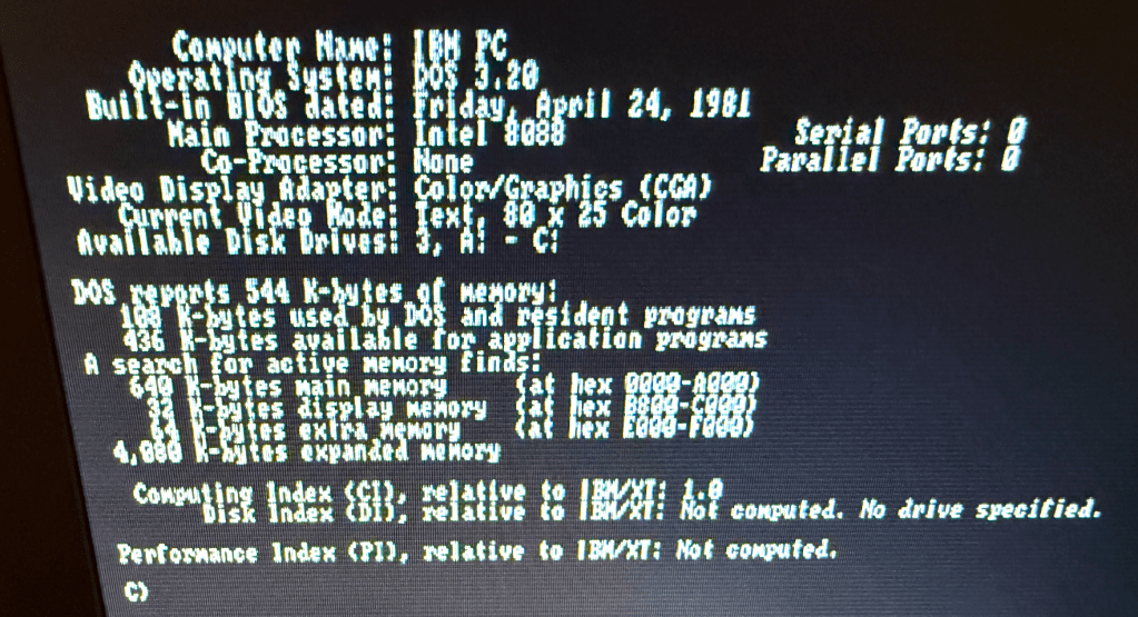
I picked up a IBM 5150 motherboard from the Silicon Valley Electronics Flea Market a a few weekends ago which appeared to be in very good condition.

I powered it up with just the power supply, VGA card, and the speaker to see if it could POST, but unfortunately it could not. Well, I did hear the pulse from the speaker which, I believe, means at least some of the BIOS was running.

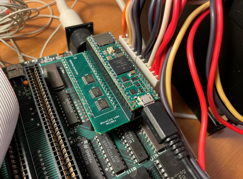
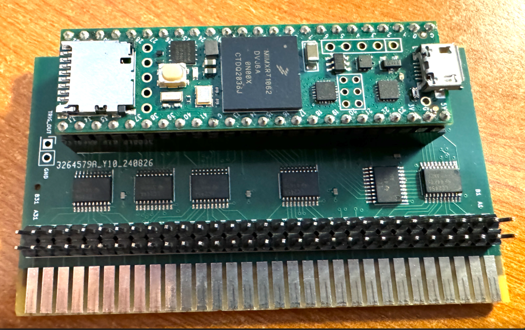
To help debug this I plugged in an MCL86+ board, or more precisely, the MCLV20_Max which shares the same hardware and got the same results as the 8088.

I then wrote a bit of simple C code to perform a series of reads and writes to the BIOS ROM and the DRAM: I read a few bytes at FFFF:0000 and did some read/writes tests of the first DRAM bank at 0000:0000.

The ROM data at FFFF:0000 looked ok – it began with 0xEA which is the long jump. But the data returned from the DRAM was 0xFF for all DRAM banks – I checked pages 00000, 10000, 20000, 30000.

This could be caused by a number of things. The first places I looked with an oscilloscope were the control and data pins of the bi-directional data buffer between the CPU and the DRAM, then I examined the RAS, CAS, and WR_n signal.

It turned out to be the WR_n signal stuck at low. Unfortunately this signal is shared with ALL 36 DRAM chips! Any of them could have been dragging this signal down or it could have been another logic chip in this path. The first step was to pull all 27 of the socketed DRAMs but the problem persisted.

The next step was to look at the logic chips that generate WR_n starting from the ones closest to the DRAMs and working my way back. I isolated the stuck net at the output of the LS04 (inverter) so I snipped the output signal and checked it with the oscilloscope to confirm I had the right chip —But unfortunately I didn’t!

The net was still low which meant there was a short in one of the soldered-on DRAM chips or a short on the PCB.

I used an ohmmeter to see where the lowest resistance was to ground. I checked each socketed DRAM and was able to find that the lowest resistance was at the Bank-1 Parity DRAM! I thought this was strange – especially since there was no IC in the socket.

I thought I had better look under the PCB – and sure enough there was a short from the Parity DRAM’s WR_n signal (Pin-3) to the ground of bypass cap C7! It was because the factory did not clip the leads to many of the IC’s on this side of the PCB so they were long enough to touch an adjacent chip when bent over.

I clipped off the long pins and that was it! My tests were then able to read and write DRAM successfully I reinstalled the rest of the DRAMs and was also able to confirm they were all working.

The MCLV20_Max/MCL86+ made this debug much easier because the IBM BIOS doesn’t give much indication of what is wrong in situations like this. I also am using a VGA card so the diagnostic ROMs will not work.

With the MCLV20_Max I was able to write, compile, load, and run simple C code tests in minutes. I was able to isolate the issue to the DRAMs very quickly.

The IBM BIOS stops accessing DRAM as soon as it sees a failure, so it stops toggling the WR_n signal very quickly. The only way to get it to toggle would have been to constantly power cycle the machine which is both slow and stressful for the motherboard.

With the MCLV20_Max I was to hard-loop my write/read tests exclusively on the DRAM which guaranteed that the RAS/CAS/WR signals were always toggling so I could measure each IC in the signal path.

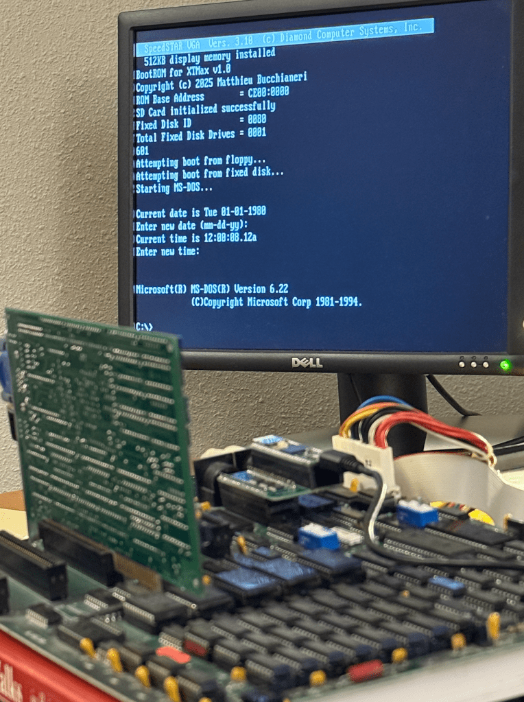
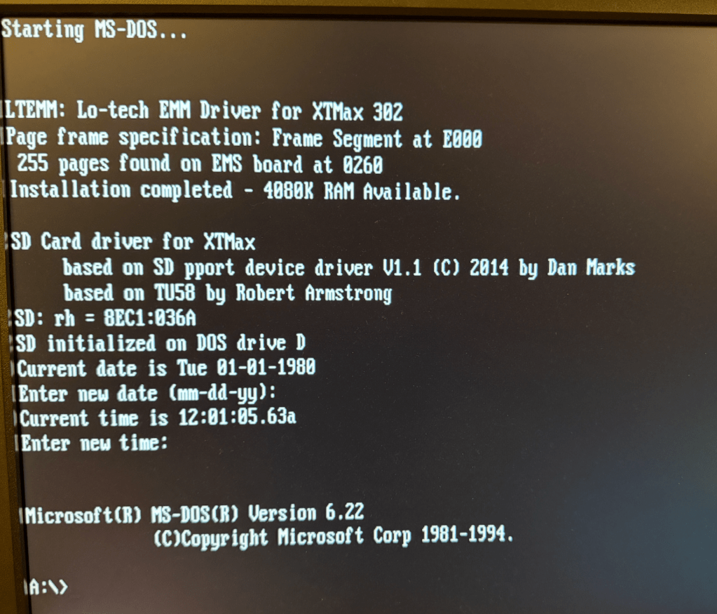
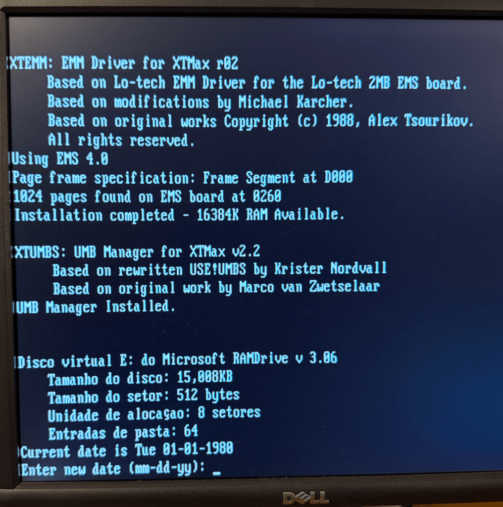
Once the debug was done I loaded in the MCLV20_Max code from GitHub in which booting from the MicroSD was recently added.

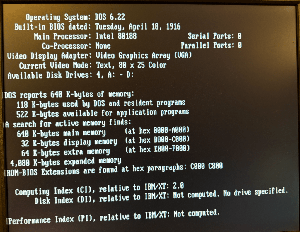
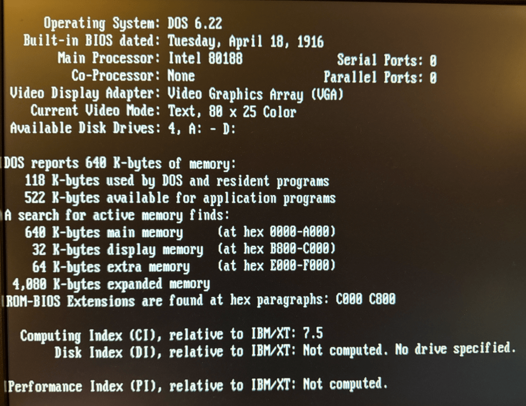
A fun fearure is that I am able to pre-set the acceleration mode to maximum so that the MCLV20_Max boots with the full 640 KB of RAM and acceleration many times faster than a stock 8088 

:)

Here it is:

MCLV20_Max / MCL86+ as a debug tool

MCLV20_Max – A Software-defined NEC V20 CPU And More

The MCLV20_Max is a Teensy 4.1-based software-defined drop-in CPU replacement for the Intel 8088 used in vintage IBM XT’s. It has enhancements built upon the MCL86+ project and uses the same PCB.

It emulates the full Intel 8088 instruction set as well as the additional 80188 and V20 opcodes. It also mimics the behavior of the V20 with its treatment of flags, shift-counts, and the ability to restart multiple prefixes upon exit of an interrupt. Below is the Anonymous BIOS which recognizes the MCLV20_Max as a V20 CPU.

In addition to the CPU emulation, some of the features of the XTMax project are integrated into the MCLV20_Max which include 4 MB of Expanded RAM and MicroSD hard drive support. Below are the drivers being loaded that configure the 4 MB of Expanded RAM and enumerate the MicroSD as drive D:

Two acceleration modes are provided. Acceleration mode 1 simply removes opcode clock cycle accuracy so that one opcode is executed for each clock. This can provide for as much as 100% speed improvement over the stock 4.77 Mhz 8088.

Acceleration mode 2 provides the maximum acceleration which can be from 5 to 10X faster than the 8088. It does this by first copying all 640 KB of the motherboard RAM plus the ROM into the Teensy’s internal memory which runs at 800 Mhz+. From then on all CPU accesses to instruction and data are handled using this fast mirror RAM with only CPU accesses to motherboard peripherals and video RAM using the CPU’s local bus. The resulting speed is faster than a 10 Mhz 80286 and approaching that of a 80386.

The MCLV20_Max also has enough internal memory to host any BIOS or diagnostic ROM.

Using a modified LoTech EMM 3.2 driver, MCLV20_Max can provide 4 MB of Expanded RAM which can be used as a fast RAMDISK and like the XTMax project, the MCLV20_Max can also provide access to a MicroSD card which is formatted as FAT16 and can be freely used by any other computer including Windows, Mac, Linux, and Chromebook.

I made a few video demonstrations of the MCLV20_Max and posted to YouTube:

All of the source code and PCB files are open source and posted on GitHub:

https://github.com/MicroCoreLabs/Projects/tree/master/MCLV20_Max

MCLV20_Max – A Software-defined NEC V20 CPU And More

XTMax – 8-bit Software-Defined ISA card using Teensy 4.1

XTMax is a software-defined 8-bit ISA card which uses a Teesny 4.1 microcontroller board that provides the functionality of THREE vintage ISA cards. It can expand “conventional” motherboard RAM up to 640 KB, adds up to 16 MB of Expanded RAM, supports 320 KB of UMB RAM, and provides bootable hard-drive access using a MicroSD card. A small PCB is used to allow nearly all of the ISA bus signals to attach to the Teensy 4.1.

A similar project to this is the PicoMem which is also a software-defined ISA expansion card, however the Teensy 4.1 used on the XTMax is nearly 3X faster than the Raspberry Pi Pico so does not share some of its limitations.

The first feature of XTMax is that it can expand the motherboard’s conventional (motherboard) ram up to 640 KB without limitation and with zero wait states. XTMax also has no limitation on the ability to support DMA to and from the computer’s floppy or spinning hard disks as PicoMem does.

XTMax can currently support 16 MB of Expanded RAM and 320 KB of UMB using a updated drivers.

XTmax also allows a MicroSD card to be accessed as a hard drive which is similar to the functionality of an XT-IDE card. By default it will be the boot device if there is no hard drive present.

All design files are open souce and posted to GitHub:

https://github.com/MicroCoreLabs/Projects/tree/master/XTMax

Here is the PCB developed using KiCAD:

And here is the actual board with a Teensy 4.1 attached:

Here is XTMax installed in a very early IBM 5150 rev-A which has 64 KB installed on the motherboard.

It shows that 4 MB of Expanded RAM was added and that the MicroSD card is accessible as the C: drive. The older IBM PC’s did not display the total amount of conventional memory, but in this application below the memory is expanded to the maximum of 640 KB.

It is worth noting that the first BIOS version of the IBM PC did not support extension ROMs and therefore do not support hard disks, so XTMax is currently the only way to have a hard disk equivalent on these machines!

Here is the total memory on this early PC as reported by Norton Utilities:

Here is a screen capture of the XTMax providing 16 MB of Expanded RAM and loads the UMB driver plus configures a 15 MB RAMDISK!

I posted a video on YouTube of the XTMax in action:

XTMax – 8-bit Software-Defined ISA card using Teensy 4.1