I would like to share an update for the MicroCore Labs MCL68+ project first introduced here: https://microcorelabs.com/2023/10/26/mcl68-motorola-68000-emulator-2/
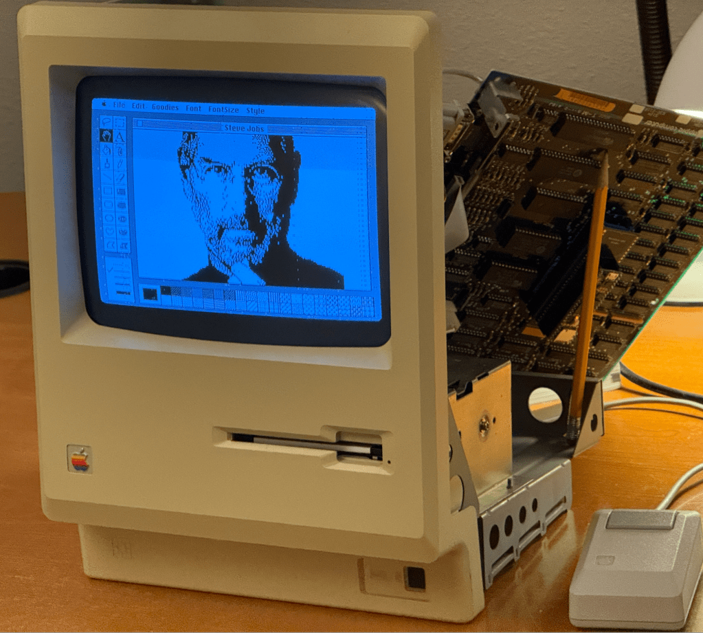
I am happy to say that it is now able to completely boot and run the Macintosh 512K!
As a winter project I thought I would pick this project back up after a two year break and see if I could make some progress. When I left off the MCL68+ was able to almost boot to the MacOS desktop but would get a fatal error.
The breakthrough was to run the MCL68+ against Tom Harte’s 68000 opcode test suite which found a number of subtle errors which were resulting in the Mac experiencing the fatal error.
The reason I did not use Tom’s test suite two years ago was because they are all written in JSON format and I lacked the skills to translate it into vectors that my code could use. I STILL lack these skills but I was able to generate the conversion code using ChatGPT. I was impressed that between my prompt and the maturity of ChatGPT it was able to generate the correct code on the first pass!
Once I had the stream of opcode before and after results I was able to plug them into the MCL68+ and see where they diverged. The errors on the MCL68+ were mainly due to incorrect effective address handling when the address for the opcode source and destination was the same register. There were a few instances of incorrect flag calculations and stack ordering as well.
I believe there were over a million tests, so I am fairly confident at this point that the MCL68+ 68000 emulation code is now mostly correct – and cycle accurate to a large degree.
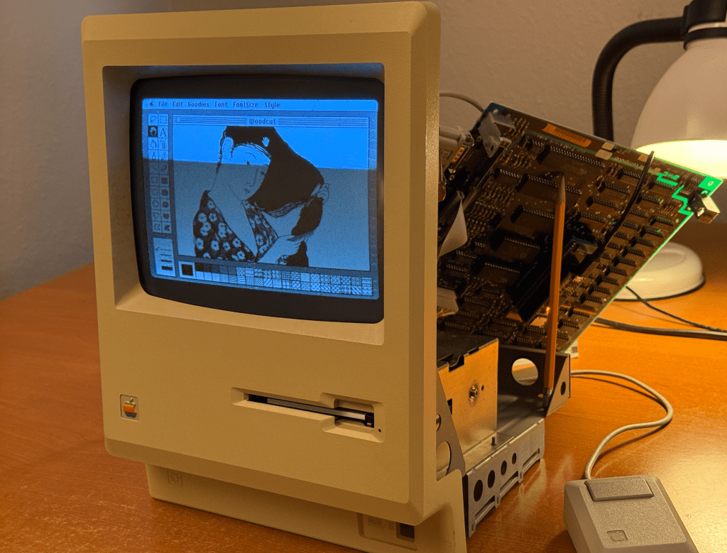
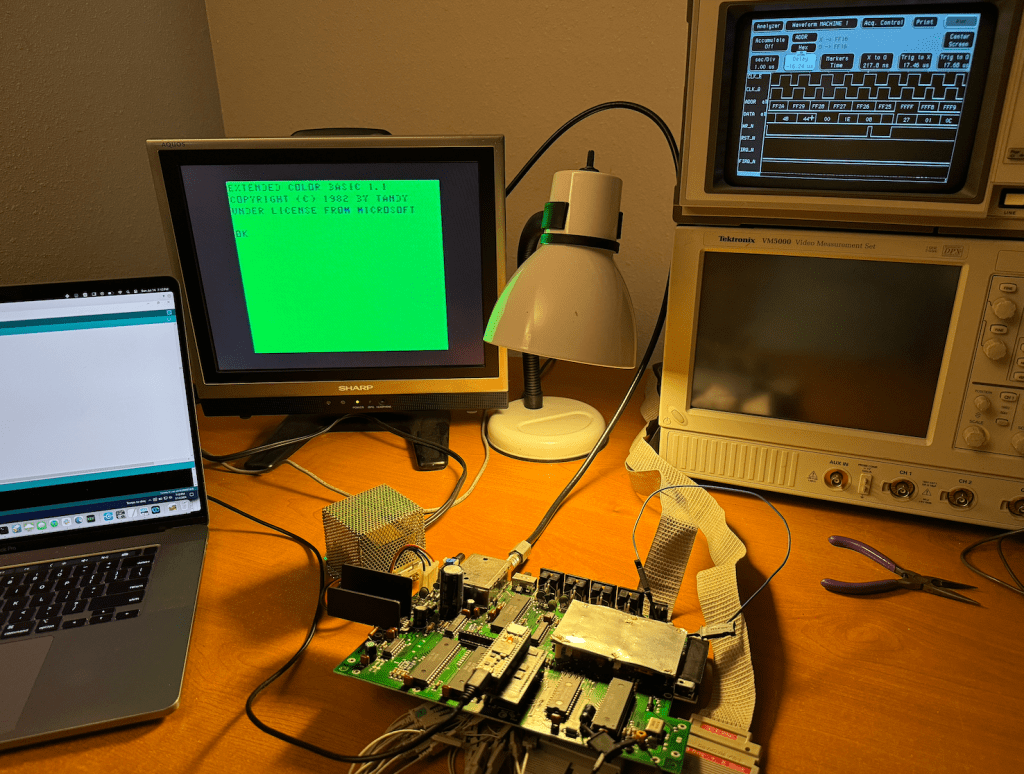
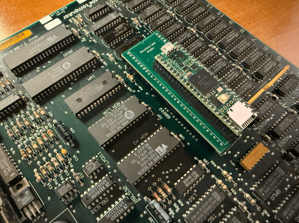
The Macintosh runs the CPU at almost 8 MHz and was a real challenge to get the Teensy 4.1 to bit-bang the local bus at that speed. I believe there are still signal integrity issues at the local bus interface so I chose to emulate the Mac’s 512K of RAM and the BIOS ROM inside of the Teensy to guarantee error-free operation. You may be able to see random dots around the screen which I believe are due to stray bus cycles writing to the video memory. These are harmless.
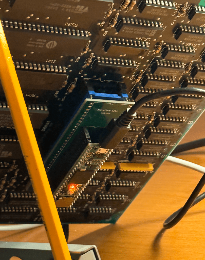
The updated source code is uploaded to GitHub: https://github.com/MicroCoreLabs/Projects/tree/master/MCL68%2B/code
Here is a short video demo of the MCL68+ running in a vintage Apple Macintosh 512K
You can reach me at: mailto:eastwood90@hush.com


")