IBM PCjr running MCL86 with “Minimum Mode” BIU.

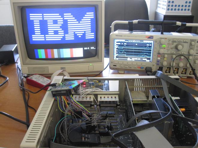
I just finished porting the MCL86 microsequencer-based 8088 core with a minimum-mode BIU (Bus Interface Unit) to a Xilinx Kintex-7 FPGA for use in an IBM PCjr!  Here are some videos of the PCjr in action:

IBM PCjr Music running on the MCL86 microsequencer based 8088 FPGA core

IBM PCjr Minuet running on the MCL86 microsequencer based 8088 FPGA core


The Xilinx Kintex-7 IOs are not 5V tolerant, so I added a Lattice ispMACH 4256ZE to translate between the Kintex and the PCjr’s motherboard.

The MCL86 core combined with the minimum-mode 8088 BIU consumes 1.5% of the Kintex-70T FPGA! Four block RAMS are used to hold the microcode.

img_4500


It is interesting to note that when I disabled the cycle-accuracy of the MCL86 core, the PCjr would no longer pass it’s POST test. It would always beep twice and then enter a HALT state.  It appears that there is a test that depends on a particular completion time. Perhaps a timer test?

What I did to bypass this was to disable cycle-accuracy until the first NMI was received which should happen either at the end of the POST when the user makes the first key-press, or when the PCjr receives the keyboard “I am OK” information during it’s POST.

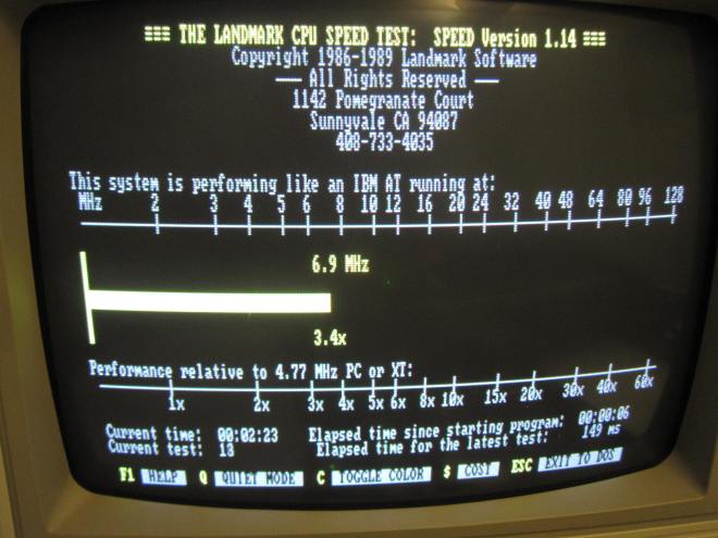
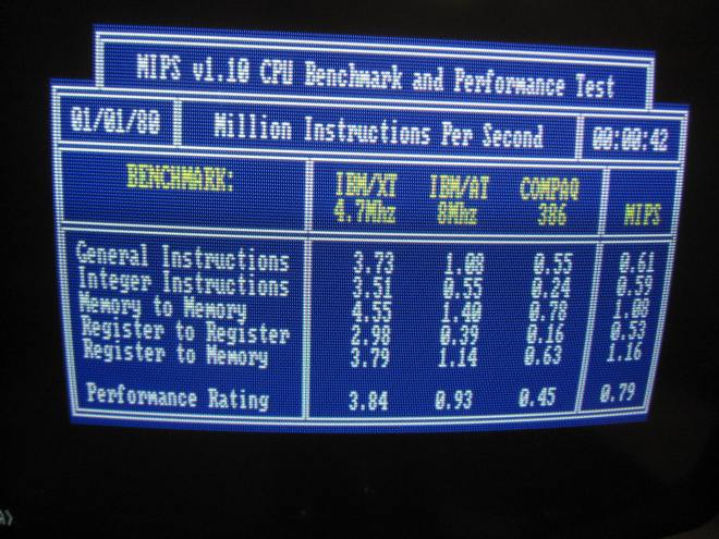
The PCjr runs noticeably faster when the cycle accuracy is disabled. The disk drive seek is faster and the warning bell when you try to use the keyboard when the CPU is busy is a higher pitch.

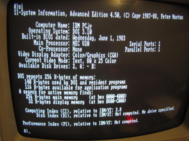
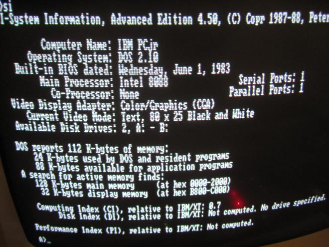
Here is the Norton Utility SI.EXE program running when cycle accuracy is enabled.

img_4484


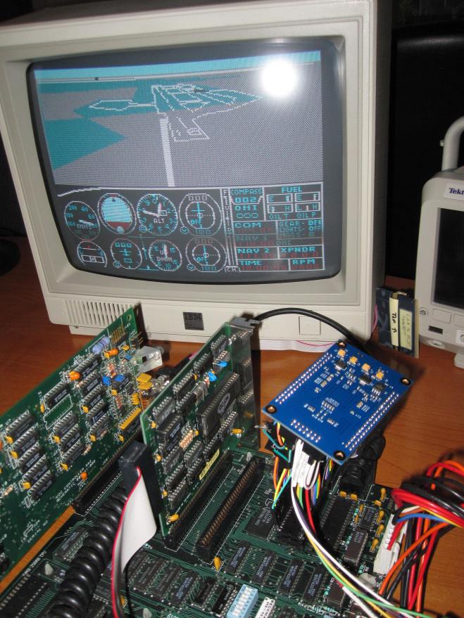
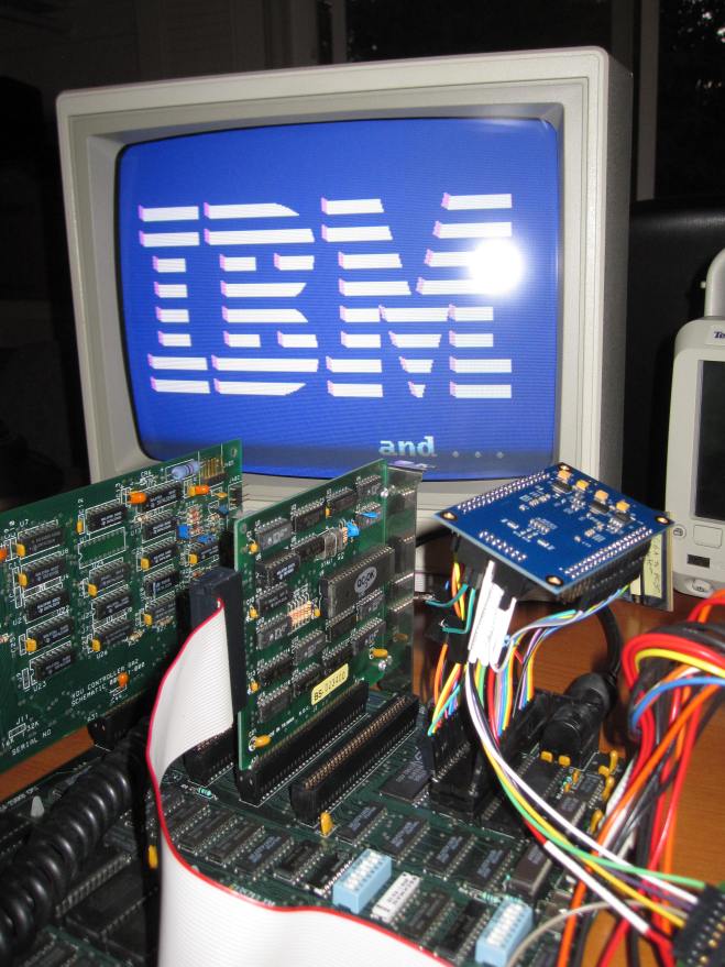
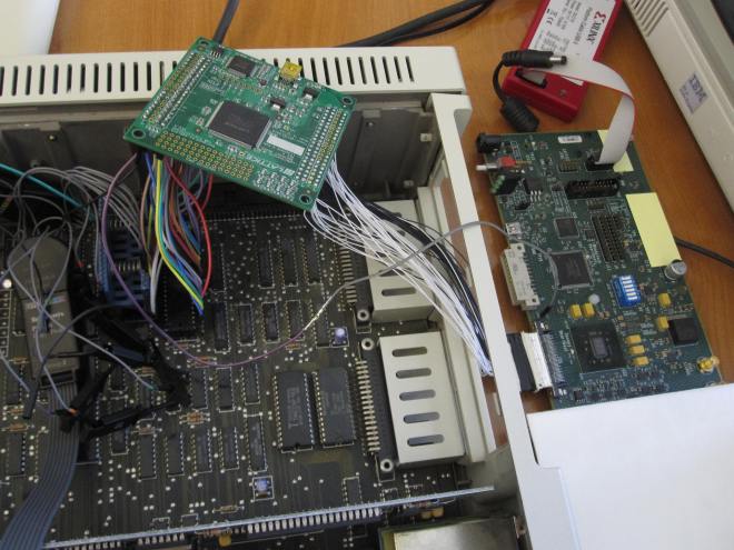
Below is a close-up of the FPGA setup. From the left there is a DIP-clip attached to the 8259 Interrupt Controller so I can probe the 8088 databus. Next to this is the 8088 adapter that is wired to the Lattice ispMACH 4256ZE breakout board which translates between the 5V motherboard and the 3.3V Xilinx Kintex FPGA. The Lattice board is wired to a board that contains the Kintex-7 FPGA.


img_4496

My next project will be to integrate some of the PCjr’s memory into the FPGA which will be accessed at the processor’s core speed to see how much performance I can squeeze out of a PCjr!  The MCL86 core is a 16-bit processor and runs at 100Mhz, so theoretically should be able to access an on-FPGA RAM more than 10X faster than memory on the motherboard!

Please visit us at: www.MicroCoreLabs.com for more information.

IBM PCjr running MCL86 with “Minimum Mode” BIU.

Lockstep Quad Modular Redundant System

Just uploaded a few vidos to YouTube of an application that uses the MCL51, the microsequencer-based 8051 core.  It is a Lockstep Quad Modular Redundant System.

There are the links:

Lockstep QMR – Artix-7

Lockstep QMR – Spartan-6

The system consists of four modules that have independent voters and the ability to rebuild themselves using data broadcast from neighboring modules. The demonstration videos show modules rebuilding themselves and rejoining the lockstep after receiving multiple types of errors that are injected into each of them.

Because the modules use the microsequencer-based MCL51 processor, the footprint is very small. The complete system consumes around 12% of a Xilinx Artix-7 xc7a35 and about half of a xc6slx9 FPGA.

img_4789

Please visit us at: www.MicroCoreLabs.com for more information.

Lockstep Quad Modular Redundant System

MCL86 running on Spartan-6

I recently picked up a Spartan-6 FPGA board from ebay (for $32!) so I thought it would be fun to load the MCL86 core and wire it up to an IBM PC 5150.  The Xilinx Spartan-6 LX9 costs close to $10 which is significantly cheaper than the $150+ Kintex-7.

Voltage dividers were used to translate between 5V and 3.3V and the FPGA’s IO drivers were set to PCI33 so the VCC clamp diodes would be enabled.  Around 10% of the FPGA’s logic was used by the MCL86 which implemented the 8088 Maximum Mode bus interface.

I read that back in the 80’s two software packages were used to judge if a computer was 100% IBM compatible. One was Lotus-123 and the other was Microsoft’s Flight Simulator. I have already run Lotus-123 successfully on the MCL86 but have not tried Flight Simulator until now.  I was not sure which version of the simulator was used, so I tried both!

Here it is:

IMG_3448IMG_3455IMG_3457

wyse_ad

Please visit us at: www.MicroCoreLabs.com for more information.

MCL86 running on Spartan-6

MCL51 Quad Core Demo

We just posted a video demonstration of a Quad Core MCL51 on YouTube:


Each core is running an independent application program.

Core-0: Parallel Port Blaster
Core-1: MIDI music player
Core-2: Sine wave generator using a R-2R DAC
Core-3: 115,200 UART Blaster

Four MCL51 8051 cores are instantiated along with a dual 24-bit timer and a UART.

A total of 1227 Artix-7 LUTs are consumed by this quad core processor which is less logic than most single core gate-based 8051 cores!

Quad_Core_Util

Please visit us at: www.MicroCoreLabs.com for more information.

MCL51 Quad Core Demo

MCL51 MIDI Player

We just uploaded a video to YouTube of the MCL51 playing “Flight of the Bumblebee” in MIDI format.  Here it is:


The program is entirely interrupt driven so the only “work” it does is either load a note into timer-0 or a delay into timer-1, after which controls passes back to the main loop. The music data takes about 2KB of Program ROM.

Below is the FPGA utilization using an Xilinx Atrix-7.  It is a little bigger than usual because we are translating the MIDI notes into thirty separate 24-bit counter registers.

Music_Utilization.JPG


Please visit us at: www.MicroCoreLabs.com for more information.

MCL51 MIDI Player

MCL51 fun with R-2R DAC

Having some fun with the MCL51 and an R-2R DAC.

We have two, eight-channel DACs made with a resistor ladder connected to the PMOD connectors of the Arty Xilinx Artix-7 test board.

The first picture uses the oscilloscope’s X-Y mode to display a 256×256 bit-mapped image.

The second and third images are made by sending the results of a lookup table to the PMOD connectors.

Please visit us at: www.MicroCoreLabs.com for more information.


IMG_3411IMG_3413IMG_3412

MCL51 fun with R-2R DAC

MCL51 Intel-Hex Loader via the UART

I just uploaded a video of the MCL51 Intel-Hex loader program. The loader is pre-programmed into the FPGA so it will always run when the FPGA is powered up. It prints a splash screen and then waits for the user to halt the CPU, load the Intel-Hex program code, and then unreset the CPU. The process from updating the user’s code, compiling, loading into the FPGA, and then running it takes a matter of seconds!


Loader


Please visit us at: www.MicroCoreLabs.com for more information.

MCL51 Intel-Hex Loader via the UART

MCL51 Testing Method

The MicroCore Labs MCL51 was tested in three stages:

During the first stage, an exhaustive set of tests was written in assembly code which would exercise each 8051 opcode and then observe the results. PSW flags were checked whether or not the instruction generated a change in their status and all four register banks were cleared and rechecked to guarantee that the opcode did not affect registers or memory outside of the intended destination. Each boolean instruction was run on multiple memory ranges that support bit-mapped operations while mathematic and string  instruction were run against all possible data values.

After these tests were developed they were run against multiple simulation tools, some of them major vendors. I was interested to find that some of the tools were not 100% correct for every 8051 instruction!  Who the vendors are and what are the errors? I’m not telling. 🙂

Once the tests were validated against multiple vendor simulators I then wired up a system to run the tests on real silicon. I chose a ROM-less 8051 variant that came in a 40-pin package and had 3.3V IOs.  This allowed be to connect it directly to an FPGA test board which you see below:


IMG_3364

The test code uses simple loops when it reaches a failure, so it was easy to run the test and simply look at the scope to see if it was running in any infinite loops. When it looped to a final address it showed that all of the tests had run successfully. The test code is nearly 6KB so it was divided into three sections and tested independantly.

After the test code was validated by known correct simulators and real silicon I was then ready to run it against the MCL51 core in my Verilog simulation environment. I am pleased that while a few subtle bugs were corrected in the MCL51 core using this test suite, I am now very confident that the core is 100% compatible and correctly implements the 8051 instruction set!

Please visit us at: www.MicroCoreLabs.com for more information.

MCL51 Testing Method

Alpha MCL51 now available

The MicroCore Labs MCL51 is now available!

The MCL51 is an ultra-small footprint, microsequencer-based, 8051 instruction-set compatible, embedded processor core that can be implemented in any FPGA or ASIC technology.

Key Features:

  • 100% Compatible with 8051 instruction set
  • Vectored interrupts with up to 128 sources
  • Proxy addressing for peripherals to allow any bus size
  • Bus Interface Unit allows high degree of peripheral customization

The MCL51 is an embedded processor core implemented with a high performance 32-bit microsequencer which utilizes less than 200 Xilinx LUTS and a single block RAM. It is 100% compatible with the classic 8051 instruction set and has a Bus Interface Unit (BIU) that provides the maximum degree of flexibility to implemented SFR registers and peripherals customized to the user’s design. Improvements to the original 8051 include up to 128 vectored interrupts as well as a proxy addressing system which allows the user to connect peripherals of any bus width to the core.

The core was run against a rigorous suite of tests which were validated using a major simulation tool as well as on genuine 8051 hardware.

Alpha MCL51 now available