Hi,
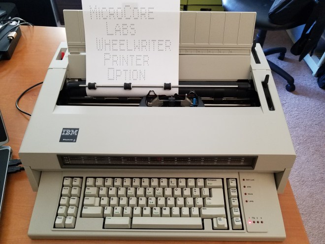
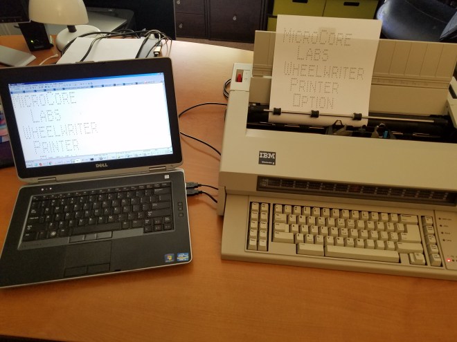
I just uploaded a small project to GitHub which is an FPGA implementation of a “Printer Option” for some of the IBM Wheelwriter typewriters. It allows the user to connect to this typewriter via a RS232 serial port. You can cut and paste into the terminal window (9600 baud) to allow using the typewriter as a printer!
Here’s the link: Wheelwriter Printer Option
And here’s a short video demonstration: FPGA Demo of Wheelwriter Printer Option
Enjoy!
-Ted
MicroCore Labs – IBM Wheelwriter Printer Option
—————————————————————————————-
Description:
————
This is an FPGA project which allows RS232 access to an IBM Wheelwriter Typewriter.
Using a terminal running at 9600 baud (9600,n,8,1), the user can directly send characters to the typewriter. They can also cut and paste long documents into the terminal, which will be printed by the typewriter. The FPGA uses XON/XOFF for flow control as well as a 1,000 character deep FIFO so that no characters are lost.
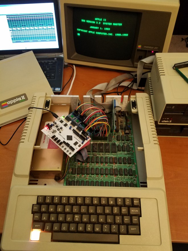
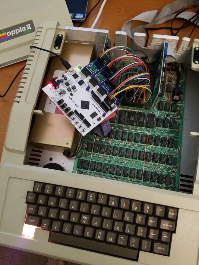
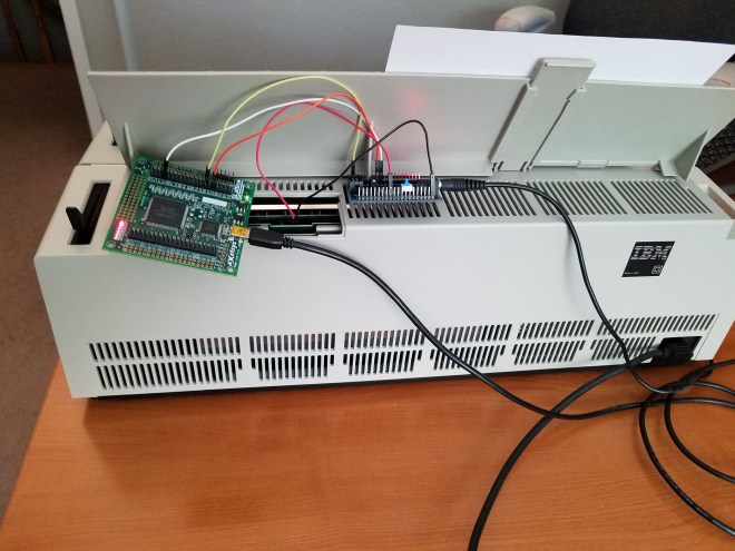
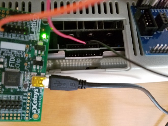
It has been tested on an IBM Wheelwriter 5, however other IBM typewriters such as the Wheelwriter 3 and 6 may also work. The only connection needed to the typewriter is via two pins within the access panel at the top rear of the typewriter.
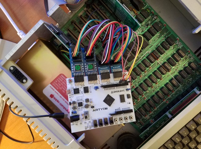
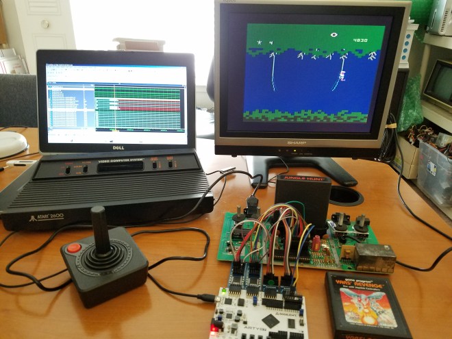
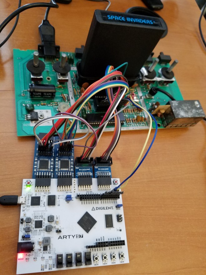
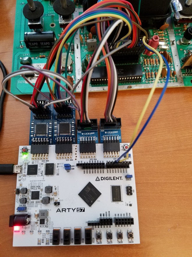
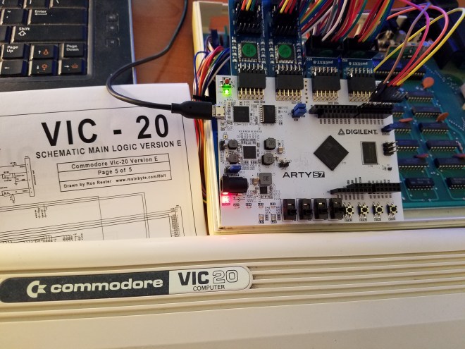
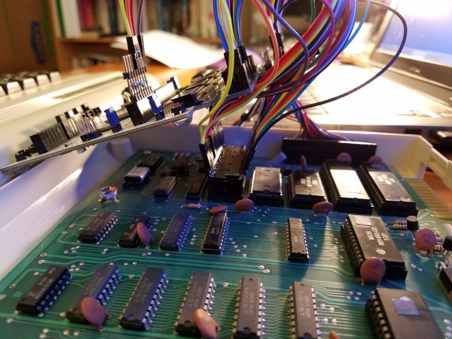
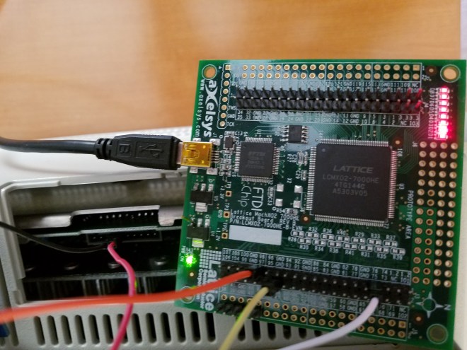
While any FPGA can be used, this project uses the Lattice XO2 Breakout Board which contains a USB interface that provides power and a RS232 serial port. To use the USB serial port, the user will need to populate the two resistors R14 and R15 which connect the RS232 TX and RX lines between the FPGA and the FTDI USB IC.
Alternatively, a second set of RS232 TX and RX pins are available which can be connected to any 3.3V compatible serial port. This was provided to allow to user to connect any type of serial port, including vintage computers. Just make sure the TTL signalling out of the converter is 3.3V to the FPGA. Both serial connections can be connected at the same time, however only one can be used at a time. In both cases, the baud rate is fixed to 9600 baud only.
Architecture:
————————
1) RS232 RX controller – fixed to 9600 baud
2) RX character FIFO – 1,000 characters deep – flags used to signal RS232 transmit of XON/XOFF
3) RS232 TX controller – fixed to 9600 baud – Used to send XON/XOFF flow control characters
4) Main Controller – Pulls new characters from the RX_FIFO and sends the appropriate command sequence to the IBM TX_FIFO
5) IBM Bus Controller – Pulls commands from the FIFO and sends them serially over the IBM_BUS
6) Bus Snooper – Used to convert IBM serial data into parallel data to be observed on a logic analyzer. Not used for the design, just for debug
Notes:
———-
– The IBM_BUS uses 5 volt logic, so a 5V to 3.3V bidirectional level shifter must be used. I used a Xilinx EPLD board,
but any technology will work that provideds this functionality.
– Both serial ports on the FPGA have light internal pullups to keep them from changing when not connected.
Pinout
——-
– The pinout for the FPGA is described in the mclwr1.lpf file
– The IBM Wheelwriter pins of interest are: 4=GND and 5=IBM_BUS. Pin#1 is on the left when looking at the typewriter from the front.